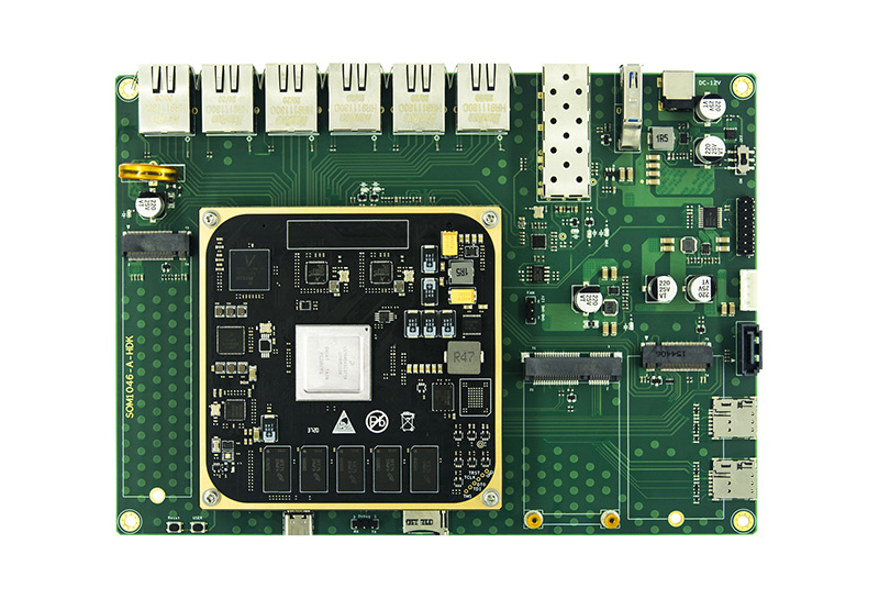
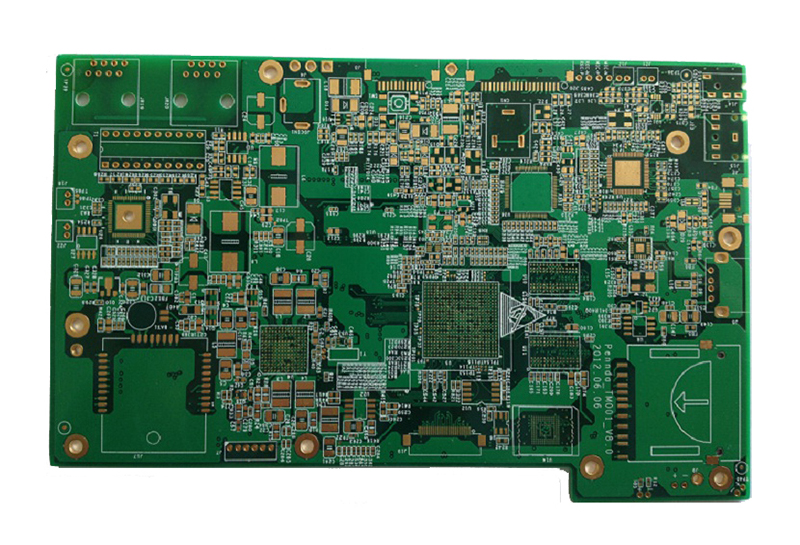
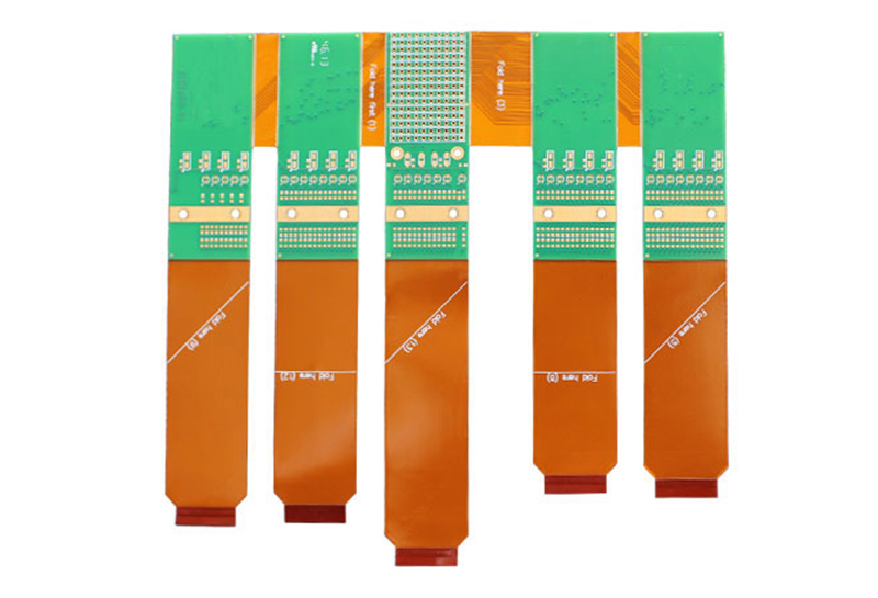
| Layers | 12 layers |
| Board thickness | 1.6MM |
| Material | Shengyi S1000-2 FR-4(TG≥170℃) |
| Copper thickness | 1oz(35um) |
| Surface Finish | ENIG Au Thickness 0.8um; Ni Thickness 3um |
| Min Hole(mm) | 0.13mm |
| Min Line Width(mm) | 0.15mm |
| Min Line Space(mm) | 0.15mm |
| Solder Mask | Green |
| Legend Color | White |
| Board size | 110*87mm |
| PCB assembly | Mixed surface mount assembly on both sides |
| ROHS complied | Lead FREE assembly process |
| Minimum components size | 0201 |
| Total components | 911 per board |
| IC packge | BGA,QFN |
| Main IC | Atmel, Micron, Maxim,Texas Instruments, On Semiconductor, Farichild,NXP |
| Test | AOI, X-ray, Functional Test |
| Application | Automotive electronics |
 With more than 10 years experience as Electronic manufacturing service provider for Telecommunication, we ANKE support various devices and telecommunication protocols: > Computing devices & equipment > Servers & routers > RF & Microwave > Data centers > Data storage > Fiber optic devices > Transceivers and transmitters
  Electronic manufacturing service provider for Automotive, we cover numerous applications: > Automotive camera product > Temperature & humidity sensors > Headlight > Smart lighting > Power modules > Door controllers & door handles > Body control modules > Energy management Layer Stackup
 Stack-up refers to the arrangement of copper layers and insulating layers that make up a PCB prior to board layout design. While a layer stack-up allows you to get more circuitry on a single board through the various PCB board layers, the structure of PCB stackup design confers many other advantages:
• A PCB layer stack can help you minimize your circuit's vulnerability to external noise as well as minimize radiation and reduce impedance and crosstalk concerns on high-speed PCB layouts. • A good layer PCB stack-up can also help you balance your needs for low-cost, efficient manufacturing methods with concerns about signal integrity issues • The right PCB layer stack can enhance the Electromagnetic Compatibility of your design as well. It will very often be to your benefit to pursue a stacked PCB configuration for your printed circuit board-based applications. For multilayer PCBs, general layers include ground plane (GND plane), power plane (PWR plane), and inner signal layers. Here's a sample of an 8-layer PCB stackup.
ANKE PCB provides multilayer/high layers circuit boards in the range from 4 to 32 layers, board thickness from 0.2mm to 6.0mm, copper thickness from 18μm to 210μm (0.5oz to 6oz), inner layer copper thickness from 18μm to 70μm (0.5oz to 2oz), and minimal spacing between layers to 3mil.
Do you guarantee safe and secure delivery of products?
Yes, we always use high quality export packaging. We also use specialized hazard packing for dangerous goods and validated cold storage shippers for temperature sensitive items. Specialist packaging and non-standard packing requirements may incur an additional charge.
How about the shipping fees?
The shipping cost depends on the way you choose to get the goods. Express is normally the most quickest but also most expensive way. By seafreight is the best solution for big amounts. Exactly freight rates we can only give you if we know the details of amount, weight and way. Please contact us for further information.

